Fabrication Facilities
-
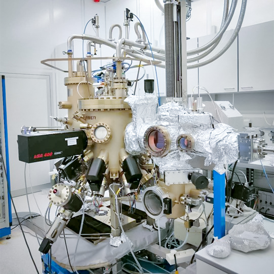
Molecular-beam epitaxy system
Type: Material growth equipment
Function: The system can grow atomically flat thin film and nano-structures of semiconductors in ultra-high vacuum environment.
-
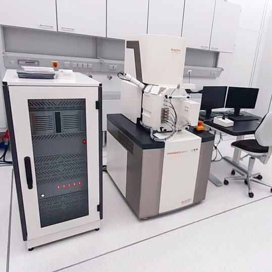
Electron-beam lithography system
Type: Material fabrication equipment
Function: The system can draw designed shapes on a surface covered with resist. The pattern of resist that can subsequently be transferred to the substrate material by etching.
-
ICP-RIE
Device for Reactive Ion Etching (RIE) with Inductive Coupled Plasma (ICP) Source for Cl and F chemistry (OXFORD RIE).
RIE technique combines isotropic chemical etching and anisotropic physical etching (sputtering).
- RIE: control on ion energy and ion density, but not independently.
- ICP: control on ion density
- ICP-RIE: independent control on ion density and ion energy.
-
HHV Thin Film Deposition System
HHV Thin Film Deposition System ATS 500 - Evaporation
- Telemark multi pocket electron beam evaporation source
- 6 crucibles of 7 cc volume each (used with 4cc liners)
- 270° beam deflection
- 6kW power rating
- X-Y beam sweep coils
- Plug-in emitter assembly
- Ultimate vacuum < 2 x 10⁻⁷ mbar
- Sample holder up to 6” wafer
- 360° sample rotation, variable rotation speeds in the range 20 to 60 RPM
- Quartz lamp substrate heater up to 250 °C
- Film thickness measurement via quartz crystal sensor
- Evaporation materials (for the moment): Au, Ti, Cr, Ni, Ge, SiO2
-
Atomic Force Microscope
Atomic Force Microscope (Nanosurf CoreAFM)
Easy-to-use AFM for research.
Measuring modes:
- Static Force Microscopy
- Lateral Force Microscopy
- Standard Spectroscopy
- Standard Lithography
- Dynamic Force Microscopy
- Phase Contrast Microscopy
- Force Modulation Mode
- MFM
- Liquid Imaging
- „QuickPrescan“, Up to 8 times faster and tip-saving image previews
- Kelvin Probe Force Microscopy (KPFM)
- Piezoresponse Force Microscopy (PFM)
-
Die Bonder
The T-4909-AE is a versatile manual die bonder designed for precision microelectronics assembly. Featuring Tresky’s True Vertical Technology™, it ensures accurate chip placement with ±10 µm precision and 95 mm Z-movement. Key features include a touchscreen interface, force control, optional tool heating, and compatibility with various bonding techniques like epoxy and flip-chip. Modular and customizable, it’s ideal for R&D labs and small-scale production. Its integrated high-definition camera and LED illumination enhance usability and alignment accuracy.
Optics Labs
Cryostats
-
Montana system
Type: Characterization setup
Function: The setup can provide a stable measurement environment from 3.2K to 350K with low thermal fluctuations and nanometer level vibrations.
-
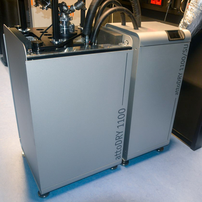
attoDRY800 system
Type: Characterization setup
Function: The system can provide a stable measurement environment from 3.8K to 320K and the magnetic field on sample to 9T.
-
attoCube800 system
Type: Characterization setup
Function: A mobile cryostation with an integrated optical breadboard. Can cool down to 3.8K.
Lasers
-
M Squared laser system
Type: Laser
Function: The system can produce continuous-wave, ultra-narrow linewidth laser from 725nm to 975nm.
-
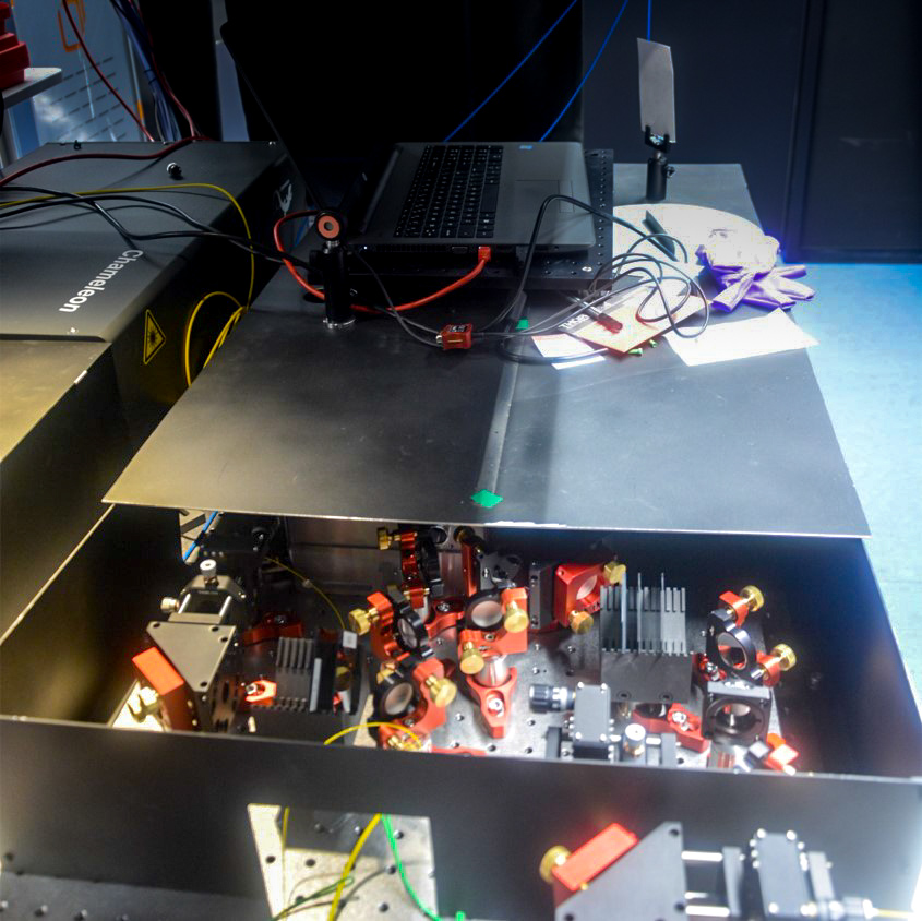
Coherent laser system (Chameleon)
Type: Laser
Function: The system can produce pulse laser from 680nm to 1080nm with the width of 140fs.
-
Coherent laser system (Mira + OPO-X)
(copy 2)
Type: Laser
Function: This modelocked laser system can generate ~2ps pulses over a wide wavelength range from 1000-1600nm at 76MHz. It can be frequency-locked to an external 76MHz reference.
-
Hübner CWave laser
Type: Laser
Function: Using SHG and parametric downconversion, this CW laser system covers a large wavelength range from ~500 to ~3300nm.
Characterization equipment
-
White light image setup
Type: Characterization setup
Function: The setup can take white light images of small structures with the resolution of several micrometers.
-
Michelson interferometer
Type: Characterization setup
Function: The setup can measure the coherent time of the incident light, operating at the wavelength around 780nm.
-
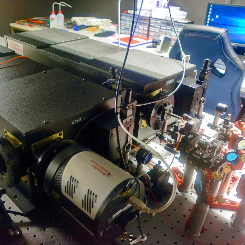
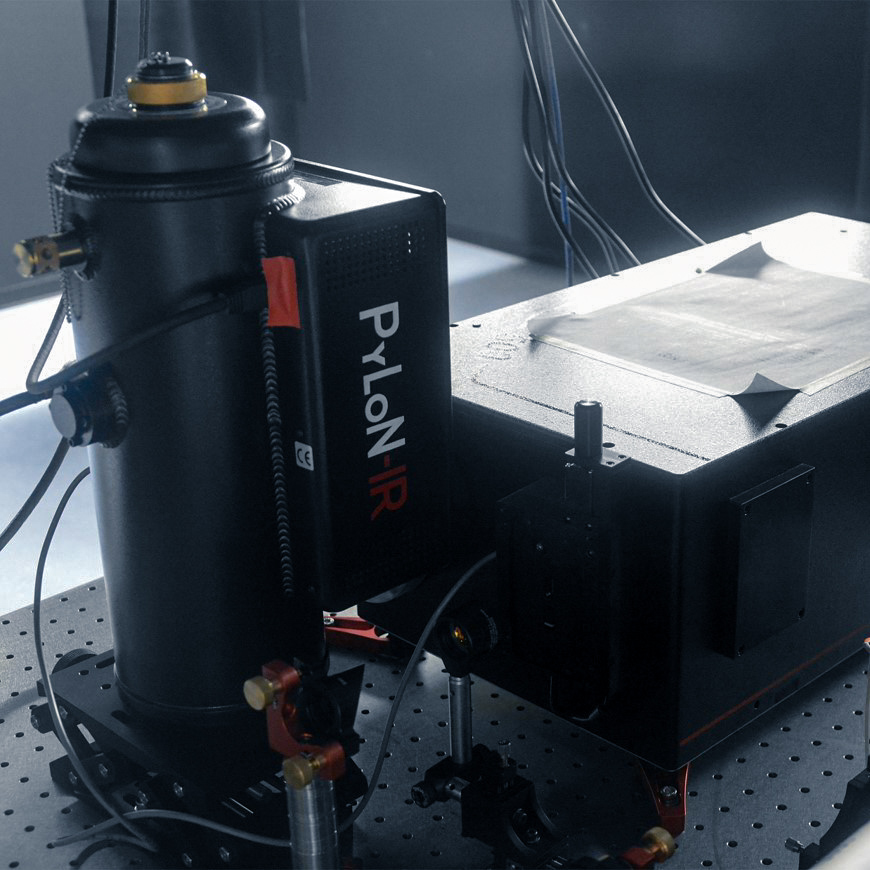
Single spectrometer
Type: Characterization setup
Function: The setup can take spectrums of the incident light.
-
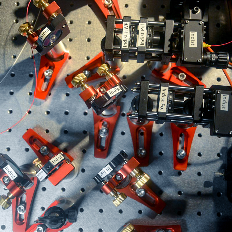
Indistinguishability setup
Type: Characterization setup
Function: The setup can measure the indistinguishability of the incident light with the wavelength around 780nm.
-
Double spectrometer
Type: Characterization setup
Function: The setup can take spectrums of the incident light and has a higher resolution compared with the single spectrometer.
-
Telecom-wavelength spectrometer
[Translate to English:] Type: Characterization setup
Function: The setup can take spectrums of the incident light at telecom-wavelength with high efficiency.





![[Translate to English:] AG Ding](https://www.fkp.uni-hannover.de/fileadmin/_processed_/d/0/csm_______4-2_dba8cfc247.jpg)
![[Translate to English:] AG Ding](https://www.fkp.uni-hannover.de/fileadmin/_processed_/d/0/csm_______4-2_74a27cf6b8.jpg)
![[Translate to English:] AG Ding](https://www.fkp.uni-hannover.de/fileadmin/fkp/AG_Ding/Labore/______4-2.jpg)


