Two-dimensional (2D) materials are subjects of current research and are of growing interesting for applications. Alongside the most known 2D material graphene there are other groups such as transition metal chalcogenides of the form MXa with Mo, W, Hf, Zr, Ti or Nb as commonly used transition metals (M), S, Se or Te as chalcogenides (X) and stoichiometry factors (a) of 2, 3 or 5. Additionally, combinations of transition metal thiophosphate or transition metal selenophosphate like Fe2P2Se6 or Cd2P2S6, hexagonal black phosphor (BP) or hexagonal boron nitride (hBN) are possible. All of these layered materials exist in 3D structures due to weak van der Waals bonding, making it is easy to separate individual layers down to an atomic scale. Some of the exotic materials show unique electrical, optical or mechanical properties. Their properties depend on the number of considered layers and can be altered by using a combination of different materials (hetero structure) or with a rotational mismatch between two layers.
Graphene Nanostructures
The atoms of carbon can bond together in diverse ways, resulting in various allotropes of carbon. The best-known forms of appearance are graphite and the diamond structure. The difference of these structures is given by their different bondings. Graphite structures have a sp3 hybridization, which means these materials have a strong layer stability while they have a weak bonding between individual layers. Ultrathin layers of carbon atoms, called graphene, provide the possibility to study freestanding two dimensional systems.
Due to their hexagonal lattice structure, monolayer graphene exhibits extraordinary properties including a Dirac type bandstructure in the vicinity of the neutrality point. The carrier concentrations in graphene can be tuned from electrons to holes.
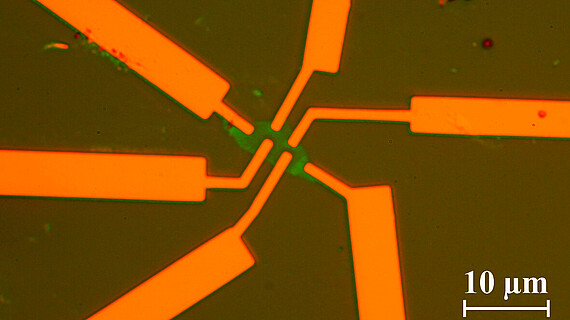
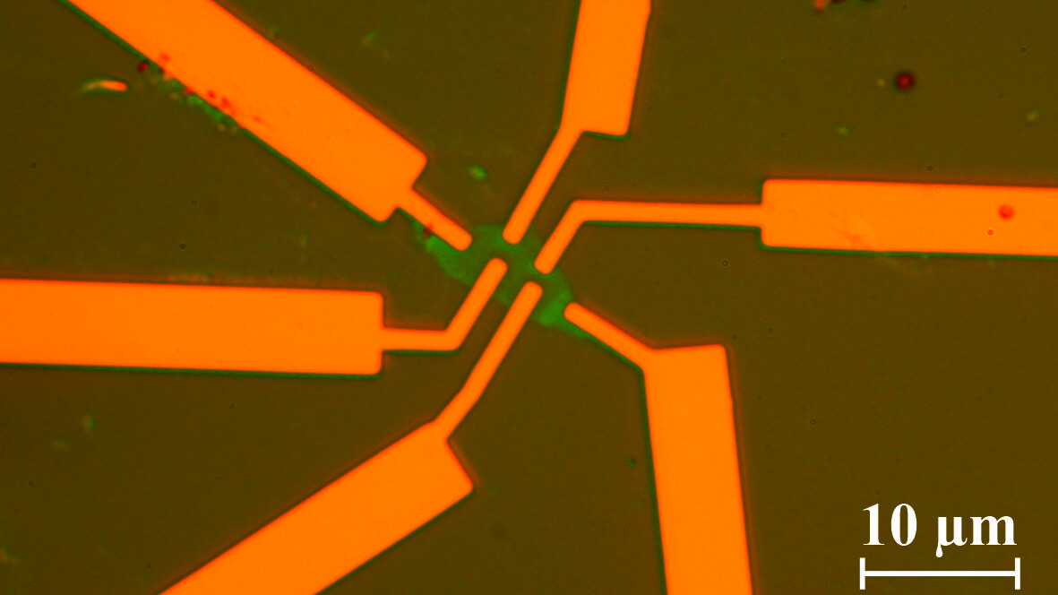
In our group single, bi- and multilayer graphene samples are prepared and investigated using magneto transport measurements and atomic force microscopy. E-beam lithography is used to define certain areas in which the graphene is etched away with a reactive oxigene plasma. The remaining parts form devices such as Hall-bars or ring-like structures in which electronic transport is investigated.

 ©
AG Haug
Atomic Force Microscopy Techniques to Generate Twisted Bilayer Graphene
The electronic properties of bilayer graphene strongly depend on relative orientation of the two atomic lattices. The rotational mismatch between both layers opens up a whole new field of rich physics, especially around the magic angle.
Twisted bilayer graphene can be obtained by different methods. We use atomic force microscopy techniques to generate twisted bilayer graphene. In this technique a diagonal cut is applied at high contact force through a monolayer graphene. Several folds spread from the newly created edge. The self-assembled twisted bilayer graphene is separated in folds with one or two rips.
Transfer of 2D Materials
We use a transfer technique which is based on the weak van der Waals force of our materials to manufacture several heterostructures of different 2D materials. For this we transfer and relocate single layers of our materials with the help of a thin film of polypropylene carbonate (PPC) and temperature variation. This transfer method is commonly used to encapsulate graphene with hBN.
Hafniumpentatelluride
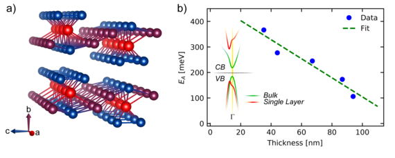
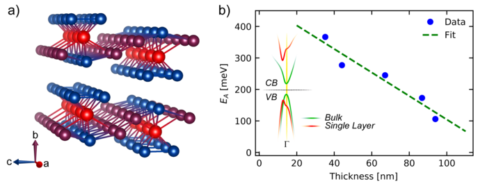
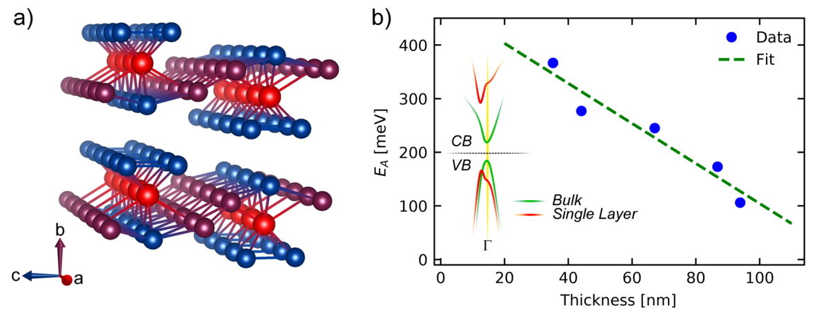
Another 2D material is e. g. hafniumpentatelluride (HfTe5) which is stacked along the crystallographic b-axis. Figure b) shows its crystal structure: 3 Te atoms (blue) are covalent bonded with one Hf atom (red) and show quasi one-dimensional channels along the a-axis which are connected to two additional Te atoms (violett) along the c-axis. Based on this asymmetrical crystallographic orientation, anisotropic physical properties are observed. In figure b) it can be seen that the band gap energy EA depends on the number of layers caused by changes in the band structure (see inset). The bulk material shows a small band gap (green) which increases by decreasing the number of layers (red). CB: Conductive Band, VB: Valence Band.
 ©
AG Haug
Contact


30167 Hannover


30167 Hannover


